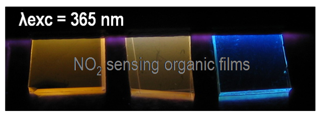
PHODYE is a multidisciplinary project that aims to develop a new sensing and recognition technology based on the integration of dye thin films with photonic structures. The developed devices should yield a distinct optical response according to changes in the environment that can be easily measured by a photonic chip or recognized directly by the human eye. The dye thin films will be prepared by a new plasma polymerization procedure that is fully compatible with the integrated optoelectronic technology. The dye molecules in the films react to changes in the concentration of certain gases and/or in temperature or UV radiation by a change of their absorption/fluorescence properties. By the use of photonic resonant structures an enhancement of the dye response is obtained achieving sensitivities below 10 ppm (NO2 detection) with a response time lower than 2 minutes. A key feature of the project is to achieve an effective optical coupling between the photonic structures and the film fluorescence/absorption response, so that changes in this latter can be transformed into proportional photonic signals or visible colour shifts.
A first technological objective of PHODYE is the integration of more than one sensing element into a chip based on ring resonators that would be capable of monitoring simultaneously various gases/physical parameters. A second technological objective is the construction of recognition chips that upon light excitation have a predetermined fluorescence response which changes depending on a given physical or chemical parameter. If subwavelenght grating structures are used, the light excitation can be ambient light and the change in the sensor response should be easily seen by the human eye as strong colour shifts.
As the optical structures have dimensions of the order of 100nms, the sensor response should be very fast. Such devices could be used as stand alone, disposable low cost sensors. Devices based on photonic resonant structures can be easily integrated into measurement devices, communication networks etc. Their low cost and their compatibility to dangerous environments where electricity cannot be used make them a unique solution for a wide range of application areas (homes, hospitals, industry, explosives, traffic, etc.).
PHODYE is intended by a consortium that integrates four research centres and three SMEs companies that cover all the scientific-technological chain from the materials to the final devices. Manufacturing, packaging, testing and validation are also afforded by the partners.
PHODYE project achievements:
The PHODYE project has been able to develop a novel sensor technology based on the photonic detection of environmental changes. The technology has been proved successful to measure the concentration in air of certain pollutant gases like NO2, the level of UV irradiation or the temperature. Encapsulated visual tags and photonic chips have been developed based in a new kind of photonic dye thin films also developed in the project.
In parallel, a cheap and reliable detection platform has been constructed and tested in real scenarios proving the good performance of the PHODYE chips. A first assessment of this new sensing technology, of its cost and of its possible uses has demonstrated that it can be competitive with some of the detection systems available in the market. NO2 visual dosimeters and monitoring systems have been recognized as application products where the developed technology is more promising. Other sensing elements are being under development following a similar strategy.
PHODYE project in brief:
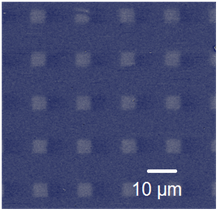
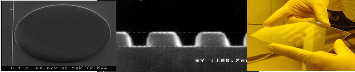
-Novel technology for the wafer-scale fabrication of luminescent nanometric organic thin films and their integration in photonic structures.
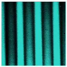
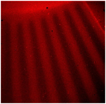
-Demonstration of room temperature sensing using the novel organic thin films in combination with three types of resonant photonic structures.
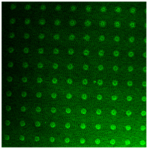
-Wafer-scale development of visual sensor integrating the luminescent films in subwavelength grating.
-Development of wafer scale packaging process compatible with ultrathin organic thin films.
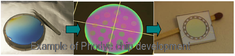
-Cost-effective fabrication and testing technologies of photonic chips that integrates all the structures for detection.
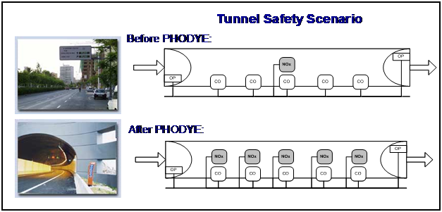
-Testing of photonic chip prototypes in real scenarios including a traffic tunnel in Valencia (Spain).
|
 Reserved Area


